E-ISSN:2583-2468

Research Article

Microwave Absorber

Applied Science and Engineering Journal for Advanced Research

2022 Volume 1 Number 5 September
Publisherwww.singhpublication.com

Ultrathin Polarization Insensitive Multiband Metamaterial Microwave Absorber for C, X and Ku Band Applications

Sood D1*
DOI:10.5281/zenodo.10984018

1* Deepak Sood, University Institute of Engineering and Technology and Kurukshetra University, Haryana, India.

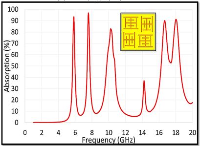
A polarization independent multiband metamaterial microwave absorber is designed and characterized. The absorber design comprise a 0.03 mm thick copper metallic pattern arranged in fourfold symmetric manner to complete one unit cell. Each metallic pattern is designed using multiple strip resonators of different lengths connected together. The top layer is separated by 1.56 mm thick FR4 dielectric from back annealed 0.03mm thick continuous copper plate. The simulated responses derived using HFSS shows that the intended absorber exhibits five absorption peaks at 5.9 GHz, 7.8 GHz, 10.9 GHz, 17 GHz and 18 GHz. with an absorption of 92.5%, 99%, 83%, 90% and 91% respectively. The electrical dimensions of the unit cell are 0.314λ × 0.314λ computed at 5.9 GHz. The designed structure is polarization independent due to four-fold symmetric design configuration and therefore exhibit the same absorption response for both TE and TM polarizations for normal incident of the EM wave. The absorption response for oblique incidence angles has also been examined for both polarizations and the absorber exhibit above 80% absorption at oblique angles of incidence. The multiband absorption make it a potential candidate for various RF applications such as RCS reduction, EMI shielding etc.

Keywords: metamaterial absorber, multiband, ultrathin, microwave absorption

Corresponding Author How to Cite this Article To Browse
Deepak Sood, , , University Institute of Engineering and Technology and Kurukshetra University, Haryana, , India.
Email:
Sood D, Ultrathin Polarization Insensitive Multiband Metamaterial Microwave Absorber for C, X and Ku Band Applications. Appl. Sci. Eng. J. Adv. Res.. 2022;1(5):15-20.
Available From
https://asejar.singhpublication.com/index.php/ojs/article/view/94

Manuscript Received Review Round 1 Review Round 2 Review Round 3 Accepted
2022-08-01 2022-08-25 2022-09-14
Conflict of Interest Funding Ethical Approval Plagiarism X-checker Note
None Nil Yes 10.12

© 2022by Sood Dand Published by Singh Publication. This is an Open Access article licensed under a Creative Commons Attribution 4.0 International License https://creativecommons.org/licenses/by/4.0/ unported [CC BY 4.0].

Introduction

Metamaterials are artificially designed sub-wavelength periodic structures that possess exotic characteristics not found in nature [1]. Their properties primarily depend on shapes and sizes of artificial accrual of resonant patterns but not on their intrinsic properties. Due to their exotic characteristics metamaterials concepts are applied to Cloaking [2], Phase Shifters [3], Filters [4] Perfect Lens [5], metamaterial transmission lines [6], Antennas [7], Perfect Absorbers [8-10], and THz waveguide [11] etc. Traditional EM absorbers such as Salisbury and Jaunmann [12] have limitations of being thick and bulky. In comparison to conventional EM absorbers metamaterial absorbers have some advantages, such as almost perfect absorption, ultrathin thickness, cost effective fabrication, light weight and compact size. Afterwards, various designs of metamaterial absorbers have been reported and investigated. Efforts have been done to design multi-band and broadband MMAs using coplanar structures and stacking of multiple layers [13, 14]. However, these approaches limits their applications due to their large size and thickness, and complexity involved in designing multiple resonant configurations. Further, higher-order resonance modes are used to design multiband absorbers using single patterned resonant structure [15, 16]. In continuation of this here a novel multi-resonant design of a five-band absorber using connected resonating strip structure with a compact unit cell is designed, and its performance is verified by simulation and experiment. Absorber exhibits above 90% absorption at five distinct resonance frequencies due to generation of higher-order resonance modes in a single resonator structure under normal incidence of EM waves. Polarization-insensitivity and oblique incidence angle behavior for both TE and TM waves is verified by through simulation. Experimental verification of absorption response for normal incidence is also performed.

Design and Simulation

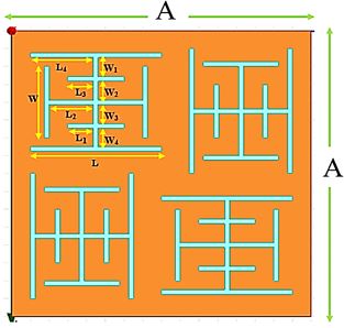
Top view of proposed multi-band metamaterial absorber is shown in Fig. 1. Top layer of absorber is made up copper metallic pattern arranged in fourfold symmetric manner to complete one unit cell. Each metallic pattern is designed using multiple strip resonators of diffe. lengths connected together.

The top and bottom layers are made up of copper with a thickness of 0.03 mm and both are separated by an FR-4 dielectric substrate having a thickness of 1.56 mm.

asejar_94_01.jpg
Figure 1:
Top view of the designed multiband absorber

The geometric parameters of proposed structure are as: A=16 mm, W = 4 mm, W1=W2=W3=W4= 1.0625 mm, L= 7 mm, L1 = L3 = 1.375 mm, L2 = 2.375 mm, L4 = 3.375mm. The structure is designed and simulated using Ansys HFSS with periodic boundary conditions and Floquet port excitation. The simulated absorption is shown in Fig. 2 and the absorption A(ω) is calculated by using Eq. 1.1 where |S11|2 is reflected power and |S21|2 is transmitted power.

A (ω) = 1 – |S11|2 -|S21|2   1.1

asejar_94_02.jpg
Figure 2:
Simulated absorption response for normal incidence of EM wave


asejar_94_03.jpg
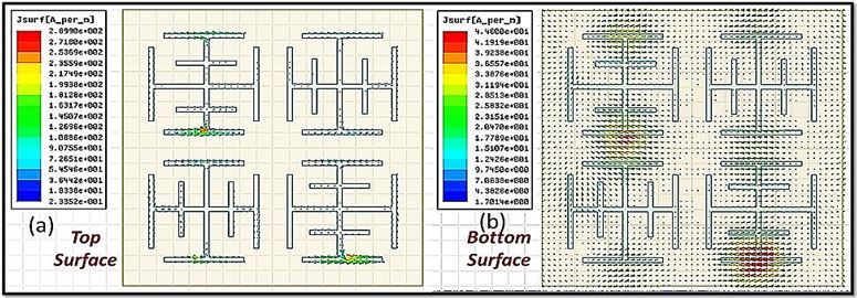
Figure 3: (a) Surface current distribution on Top Layer (b) Surface current distribution on Bottom Layer

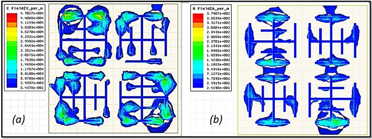
Fig. 3 (a) and (b) show the surface current distribution at the top and the bottom layer at the resonant frequencies. The current distribution on both layers is anti-parallel which forms current loops and these current loops form magnetic resonance inside the metamaterial absorber. The overlapping of the magnetic and electric resonance causes electromagnetic absorption.

asejar_94_04.jpg
Figure 4: (a) shows the electric field distribution and (b) shows the magnetic field distribution

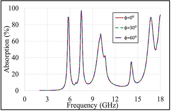
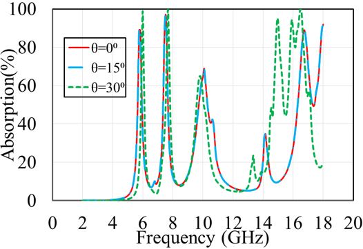
The designed metamaterial absorber is also tested for various polarization angles as shown in Fig. 5. As the design is fourfold symmetric therefore,the absorption remains same for all polaization angles. The simulated response of the absorber for different oblique angles of the incident wave under TE polarization is shown in Fig. 6. It is observed that the design exhibit angular insensitivity as the absorption is least affected under oblique angles of wave incidences.

asejar_94_05.jpg
Figure 5:
Simulated absorption response for different polarization angles

asejar_94_06.jpg
Figure 6:
Simulated absorption response for different oblique angles under TE Polarization

Experimental Results

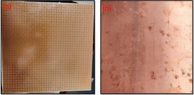
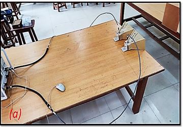
The designed metamaterial absorber was experimentally tested by a 19×19 unit cell having dimensions of 304×304 mm. Fig. 7 shows the fabricated prototype of the designed structure. The design is fabricated using PCB (Printed Circuit Board) technology. The experimental setup is shown in Fig. 8(a).


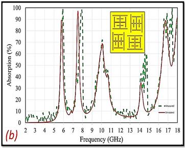
Measurements was performed by using Vector Network Analyzer (PNA series N5222A) which was connected to the two horn antennas for transmitting and receiving electromagnetic waves ranging from 2 GHz to 18 GHz. The experimental results showed multiband absorptivity ranging from 5.9 GHz to 17.44 GHz.

The Fig. 8(b) shows a comparison of simulated and experimental results and it is observed that both are almost similar. Minor differences in both results can be caused by fabrication tolerance and environmental conditions.


For normal incidence TE polarization response, the designed structure was rotated along with the x,y directions, and the angle of incidence was kept constant along with the z direction and the absorption peaks were observed at 5.9 GHz, 7.87 GHz, 10.96 GHz, 13.28 GHz, 17.04 GHz, and 17.44 GHz.

Then designed structure was tested at a 45° incident angle for TE polarization and absorption peaks were observed at 5.93 GHz, 7.9 GHz, and 10.96 GHz. These two polarization results showed that designed absorber is polarization-insensitive.


asejar_94_07.jpg
Figure 7: (a) Top view (304×304mm2) and (b) bottom layer of designed structure


asejar_94_08.jpgasejar_94_08b.jpg
Figure 8: (a) Experimental Setup (b) Comparison of Simulated and Experimental Results

The designed absorber was compared with the other metamaterial absorber as shown in Table 1.1. It is observed from the comparison that the designed metamaterial absorber is ultra-thin (1.6mm) with multi-band absorption. In addition, the structure was compact and polarization-insensitive.


Table 1.1: Comparison of different single layer metamaterial absorbers

ReferenceThickness (mm)Unit Cell Size (mm2)Absorption Frequency Range above 90% in GHzPolarization Insensitive
[17]27.1×7.1
0.237 λ × 0.237 λ
7.85-12.25NO
[18]3.28×8
0.293 λ × 0.293 λ
6.86–15.16NO
[19]1.544.5×4.5
0.157 λ × 0.157 λ
8.60-12.35NO
[20]1.64.4×4.4
0.165 λ × 0.165 λ
7.73-14.82NO
[21]312×12
0.53 λ × 0.53 λ
12.5-14YES
[22]830×30
1.19 λ × 1.19 λ
5.8-18YES
[23]1112×12
0.602 λ × 0.602 λ
3.9-26.2YES
[24]1.67×7
0.315 λ × 0.315 λ
10.36-16.67NO
[25]1.910×10
0.159 λ × 0.159 λ
4.78, 6.91,7.86, 9.14, 9.81, 10.86,
and 11.65
YES
Proposed Design1.616×16
0.314 λ × 0.314 λ
5.9, 7.8 , 10.9 , 17 and 18YES

Conclusion

A compact, polarization-insensitive multiband metamaterial absorber with a thickness of 1.6mm is designed. The proposed structure is composed of metallic dipoles of different lengths on the top layer and a continuous metallic layer at the back and both layers are separated by a 1.56mm thick FR-4 substrate.

The design shows simulated multiband absorption at five peaks i.e. at 5.9 GHz, 7.8 GHz, 10.9 GHz, 17 GHz and 18 GHz. with an absorption of 92.5%, 99%, 83%, 90% and 91% respectively. The surface current distribution of the top and bottom layers is studied. In addition, magnetic field and electric field distribution is also plotted.

The polarization-insensitivity of the structure was studied for normal and oblique incidence angles for TE polarization. The designed metamaterial absorber has ultrathin thickness, compact size, higher FWHM, polarization-insensitivity, and multi-band absorption. This designed structure is suitable for many applications like radar cross section reduction, stealth technology, super lens, etc.

References

1. R.S. Kshetrimayum. (2004). A brief intro to metamaterials. IEEE Potentials, 23(5), 44–46.
2. D. Schurig, J. J. Mock, B. J. Justice, S. A. Cummer, J. B. Pendry, A. F. Starr, & D. R. Smith. (2006). Metamaterial electromagnetic cloak at microwave frequencies. Science, 314, 977–980.
3. M. A. Antoniades, & G. V. Eleftheriades. (2003). Compact linear lead/lag metamaterial phase shifters for broadband applications. IEEE Antennas and Wireless Propagation Letters, 2, pp. 103-106.
4. M. Gil, J. Bonache, & F. Martín. (2008). Metamaterial filters: A review, 2, 186-197.
5. Fang, , H. Lee, C. Sun, & X. Zhang. (2005). Sub-diffraction-limited optical imaging with a silver superlens.Science, 308, 534–537.
6. A. Sanada, C. Caloz, & T. Itoh. (2004). Characterization of the composite right/left handed transmission lines. IEEE Microwave Wireless Components Letters, 14, 280–282.
7. R. W. Ziolkowski. (2006). Metamaterial-based efficient magnetically small antennas. IEEE Transactions on Antennas and Propagation, 54(7).
8. N. I. Landy, S. Sajuyigbe, J. J. Mock, D. R. Smith, & W. J. Padilla. (2008). Perfect metamaterial absorber. Phys. Rev. Letters, 100, 207402.
9. Y. I. Abdulkarim, A. Mohanty, O. P. Acharya, Bhargav Appasani, Mohammad S. Khan, S. K. Mohapatra, F. F. Muhammadsharif, & J. Dong. (2022). A review on metamaterial absorbers: Microwave to optical. Frontiers in Physics, Sec. Optics and Photonics, 10, 1-18 .
10. B. X. Wang, H. X. Zhu, & W. Q. Huang. (2019). Multiple-band ultra-thin perfect metamaterial absorber using analogy split-ring resonators. Plasmonics, 14, 1789–1800.
11. C. R. Williams, M. Misra, S. R. Andrews, S. A. Maier, S. Carretero-Palacios, S. G. Rodrigo, F. J. Garcia-Vidal, & L. Martin-Moreno. (2010). Dual band terahertz waveguiding on a planar metal surface patterned with annular holes. Appl. Phys. Lett., 96, 011101.


12. W. W. Salisbury. (1954). Absorbent body for electromagnetic waves. United States Patent 2599944.
13. G. Dayal, & S. A. Ramakrishna. (2013). Design of multi-band metamaterial perfect absorbers with stacked metal– dielectric disks. Journal of Optics, 15, 055106.
14. D. Yang, & Y. Xia. (2020). Experimental verification of multi-band metamaterial absorber with double structured layers. Materials Research Express, 7, 035801.
15. Y. He, B.X. Wang, P. Lou, & H. Zhu. (2020). Multiple-band absorber enabled by new type of metamaterial resonator formed by metallic split ring embedded with rectangle patch. Results in Physics, 18(103251), 1-5.
16. Y. J. Kim, J. S. Hwang, Y. J. Yoo, B. X. Khuyen, X. Chen, & Y. P. Lee. (2017). Triple-band metamaterial absorber based on single resonator. Current Applied Physics, 17, 1260-1263.
17. S. Ghosh, S. Bhattacharyya, D. Chaurasiya, & K. V. Srivastava. (2015). An ultrawideband ultrathin metamaterial absorber based on circular split rings. IEEE Antennas and Wireless Propagation Letters, 14, pp. 1172-1175.
18. S. Bhattacharyya, S. Ghosh, D. Chaurasiya, & K. V. Srivastava. (2015). Wide-angle broadband microwave metamaterial absorber with octave bandwidth. Aplied Physics A, 9, 1160–1166.
19. D. Sood, & C.C. Tripathi. (2015). A wideband ultrathin low profile metamaterial microwave absorber. Microwave & Optical Technology Letters, 57, 2723-2728.
20. D. Sood, & C.C. Tripathi. (2016). A wideband wide-angle ultrathin low profile metamaterial microwave absorber, 58, 1131-1135.
21. H. Zhai, C. Zhan, L. Liu, & Y. Zang. (2015). Reconfigurable wideband metamaterial absorber with wide angle and polarisation stability. Electronic Letters, 51, 1624-1626.
22. W. Li, T. Wu, W. Wang. J. Guan, & P. Zhai. (2014). Integrating non-planar metamaterials with magnetic absorbing materials to yield ultra-broadband microwave hybrid absorbers. Appl. Phys. Lett., 104, 022903.
23. Y. Shen, Z. Pei, Y. Pang, J. Wang, A. Zhang, & S. Qu. (2015). An extremely wideband and lightweight metamaterial absorber. Journal of Applied Physics, 117, 224503.

24. S. Ramya, I., & Srinivasa Rao. (2017). A compact ultra-thin ultra-wideband microwave metamaterial absorber. Microwave & Optical Technology Letters, 59, 1837-1845.
25. Y. Cheng, Y. Zou, H. Luo, F. Chen, & X. Mao. (2019). Compact ultra-thin seven-band microwave metamaterial absorber based on a single resonator structure. Journal of Electronic Materials, 48, 3939–3946.